USER CONSTRAINTS FILE
(Last Modified: 04 November 2010 06:09:16 PM )
The UCF file (User Constraints File) is used (by Xilinx tools) to place constraints on the synthesis and place-and-route tool. Most of these constraints can also be done via pragmas in the source code, but since the pragmas vary from tool to tool, placing them in the UCF file is very common (since this entire file is tool-specific)
For the typical low-end FPGA developer there are generally only two or three three types of constraints that are placed in UCF file:
To assign signals to specific pads so as to control the FPGA pinout.
To set timing constraints, the most important of which is the period of the master clock. In fact, in most fully synchronous designs, this is the only timing constraint initially and others are added only as necessary.
To set I/O options such as slew rates on individual pads. These are frequently omitted initially and, as with most timing constraints, only added as necessary.
Initially, the top level ports of the DE248 mapped to the top level logic directly. By this it is meant that if a signal named MEMDATA was brought to an FPGA pin that the UCF file mapped MEMDATA to that pin. However, as chip-specific modifications were made this proved extremely cumbersome and a source of confusion since it was difficult to resist the temptation to simply use the existing signal name even though purpose of that signal had changed radically. As a result, the UCF signal names now represent the names found in the Digilent documentation and these are then mapped to the internal DE248 signals in the top-level source code file. An advantage of this is that the UCF file does not need to be changed nor does it even need to be referenced. The signal locations can be referenced directly from the top-level code to the Digilent D2 Reference Manual.
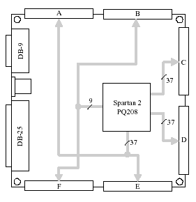
The actual port assignments can be found at the bottom of the top level Verilog code (de248.v). Each port has a buffer explicitly instantiated although the type of buffer depends on the type of signal. In each case, however, a consistent naming and use convention is used, at least for the four sets of expansion port signals. First, the instance name is of the format Pp_nn where 'p' is the port designator and 'nn' is the port pin number. Then the first assignment in the instantiation is the external signal name (the one that is mapped to a specific pin in the ucf file) while the internal signals appear last. The buffer instantiation is generally followed by a comment indicating which firmware module the internal signal is associated with.
There are presently four buffer types in use. Following is an example of each:
Output Buffer
OBUF PC_29 (.O(PortC[29]), .I(MOSI)); // SPI:MOSIThis is an output buffer servicing Port C pin #29. The internal signal is the MOSI port of the SPI module.
Input Buffer
IBUF PC_27 (.I(PortC[27]), .O(MISO)); // SPI:MISOThis is an input buffer servicing Port C pin #27. The internal signal is the MISO port of the SPI module.
Bidirectional Buffer
IOBUF PA_05 (.IO(PortA[5]), .T(MEM1_WEb),
.I(MEM1_WD[0]), .O(MEM1_RD[0]));  // MEM:D0
This is a bidirectional buffer servicing Port A pin #5. The control signal is
MEM1_WEbwhile the internal signal going out isMEM1_WD[0]and the internal signal coming in isMEM1_RD[0].
Global Clock Buffer
IBUFG PB_11 (.I(PortB[11]), .O(PortB_NC[11])); //
Global Clock Buffer
This is a global glock input buffer servicing Port B pin #11. There is no internal signal, so the input is assigned to a wire in the
PortB_NC(no connection) bus which is declared specifically for this purpose.
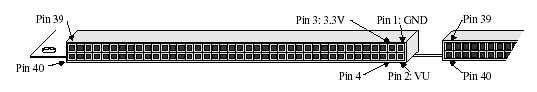
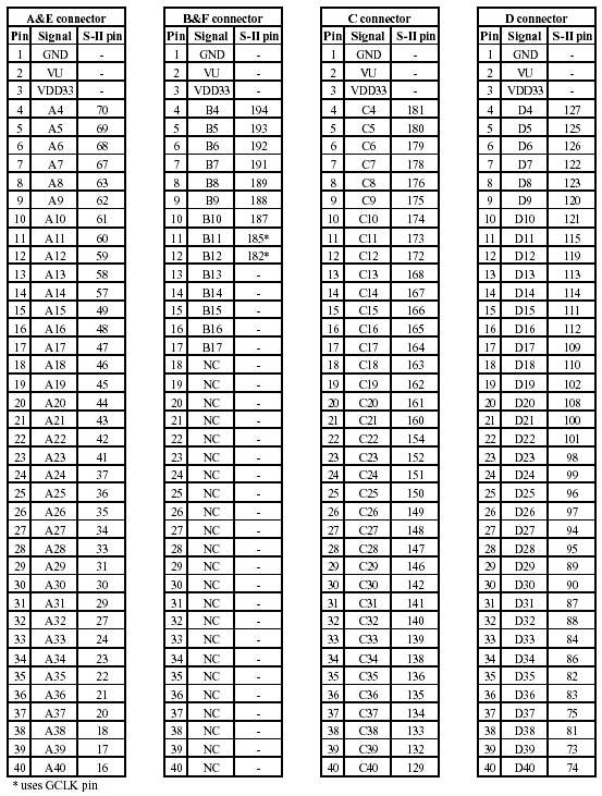
The following information is reproduced from the Digilent D2 Reference Manual for convenience.