SPI MASTER MODULE
(Last Modified: 04 November 2010 06:09:08 PM )
//
======================================================================

// SPI MASTER

// ======================================================================


// SPI Control Map

// |    7   |    6   |
5   |    4   |    3
|   2   |    1   |
0   |

// |MISO_INV|MOSI_INV| SSN_INV|SCLK_INV|FreeRun |  DIR  |  CPOL
|  CPHA  |


// External Interface

wire SCLK, SSN, MOSI, MISO;


// Test Signal Interface

wire [15:0] SPI_Test;


SPI_MASTER_phy SPI_PHY

(

    .Test8(SPI_Test[7:0]),

    .packet_RX(SPI_Packet_RX), .packet_TX(SPI_Packet_TX),

    .initiate(SPI_Initiate),

    .length(SPI_Length), .control(SPI_Control),
.clkdiv(SPI_ClkDiv), .target(SPI_Target),

    .busy(SPI_Busy),

    .MOSI(MOSI), .MISO(MISO), .SCLK(SCLK), .SSN(SSN),

    .rst(rst), .clk(clk)

);


assign SPI_Test[15] = SPI_Busy;

assign SPI_Test[14] = SPI_HOST_Source[0];

assign SPI_Test[13] = SPI_Packet_TX[0];

assign SPI_Test[12] = SPI_Initiate;

assign SPI_Test[11] = MISO;

assign SPI_Test[10] = MOSI;

assign SPI_Test[9]  = SSN[0];

assign SPI_Test[8]  = SCLK;
The SPI module implements a very flexible SPI Master device within the FPGA. The HOST can configure the module with the User's choice for the following options:
The length of the packet, from 1 bit to 255 bits.
The SPI clock rate, as a divisor of the FPGA master clock.
The SPI mode.
Orientation of data transfer (i.e., lsb or msb first).
Independently control the polarity of each external interface signal.
Whether the SPI clock is gated or free running.
Whether the SPI is controlled directly via the HOST or indirectly via the Loop Controller.
Since the FPGA register space is not initialized to any particular values, it is in general not safe to assume any default values for the contents of those registers. Hence, the User should always explicitly write the desired control values to the registers after configuring the FPGA.
The default register map places the SPI HOST registers at the following addresses:
| Register | Signal |
Description |
| HOST 0x10 | SPI_HOST_Source | SPI signal source control |
| HOST 0x11 | SPI_HOST_Packet_TX[ 7: 0] | Transmit Packet Data (LSB) |
| HOST 0x12 | SPI_HOST_Packet_TX[15: 8] | Transmit Packet Data (MSB) |
| HOST 0x13 | SPI_HOST_Length | Packet Length (bits) |
| HOST 0x14 | SPI_HOST_ClkDiv | Clock Divider value |
| HOST 0x15 | SPI_HOST_Control | Control Register |
| HOST 0x16 | SPI_HOST_Target | Targeted Slave Device |
| FPGA 0x91 | SPI_Packet_RX[ 7: 0] | Received Packet Data (LSB) |
| FPGA 0x92 | SPI_Packet_RX[15: 8] | Received Packet Data (MSB) |
The SPI module can be controlled either directly via the HOST interface or indirectly via the Loop Controller. In either case, the meaning of the signals are the same with the sole difference being the source of those signals; in particular, signals that normally come from the HOST registers are taken from SPI_LOOP_name instead of SPI_HOST_name.
This document focuses solely on the SPI as used when controlled directly via the HOST interface, therefore the registers that deal with the Loop Controller will only be discussed to the degree necessary to configure the DE248 so that the SPI module is controlled via the HOST interface. For information on running the SPI under the control of the Loop Controller, see that documentation.
|
SPI_HOST_Source |
|||||||
| 7 | 6 | 5 | 4 | 3 | 2 | 1 | 0 |
| N/A | N/A | N/A | Loop | N/A | N/A | N/A | HOST_Initiate |
When the SPI_HOST_Source register has b4 set, the SPI module is under the control of the Loop Controller and all signals are obtained from it. When this bit is cleared, the SPI is under the direct control of the HOST registers and the HOST_Initiate bit (b0) of the SPI_HOST_Source register is used to initiate an SPI packet transfer each time it is asserted. This therefore requires two writes to the register for each transfer, one to set the HOST_Initiate bit and one to clear it. The remaining bits in the register are presently unused and should be written as zeros to be safe. The HOST_Initiate bit is ignored if the SPI is under the control of the Loop Controller.
|
SPI_HOST_Length |
|||||||
| 7 | 6 | 5 | 4 | 3 | 2 | 1 | 0 |
| b7 (lsb) | b6 | b5 | b4 | b3 | b2 | b1 | b0 (lsb) |
This register sets the length of the SPI packet. The system is optimized for 16-bit packets, so normally a value of 0x10 would be written to this register. A length of zero results in no packet being sent, although possible future plans are for this to result in a 256-bit packet, which would facilitate the daisy-chaining of up to sixteen 16-bit packet slave decides.
Lengths from 1 bit to 255 bits are nominally supported, however the behavior is non-standard for lengths other than sixteen. This behavior affects the Packet Data Registers and is described there. For packets less than 16-bits in length and shifted out lsb-first, the behavior for the transmitted data is as expected and this is sufficient to work with existing BFE IC's having other than 16-bit SPI interfaces, all of which are less than sixteen bits. It is possible that, in the future, the module may be modified to properly work with other than 16-bit packets, but that will not happen until a need is identified.
|
SPI_HOST_ClkDiv |
|||||||
| 7 | 6 | 5 | 4 | 3 | 2 | 1 | 0 |
| b7 (lsb) | b6 | b5 | b4 | b3 | b2 | b1 | b0 (lsb) |
The SPI clock (SCLK) is at a frequency that is Pclk/[2(1+ClkDiv)] where Pclk is the FPGA master clock. For a master clock frequency of 50 MHz, this means that SCLK frequencies of 25 MHz down to just below 100 kHz can be realized.
If ClkDiv is set to 0, then the SCLK rate is half the Pclk rate, meaning that it toggles on each rising edge of Pclk. The SSN signals change state on the falling edge of Pclk so that the SPI protocol, which requires SSN signal changes to occur away from SCLK signal changes, can be adhered to. Some BFE chips are designed specifically to permit the two signals to change concurrently by internally delaying the SCLK signal, however the preferred solution is to adhere to the protocol.
Ideally the SSN signals would be scheduled to change midway between SCLK edges and originally this was the case (with the SSN signals changing in the rising edge of Pclk), however this limited the maximum SCLK frequency to just one-fourth of the master clock frequency, which was inadequate for the one of the target chips. The present code permits a higher SCLK rate, but the consequence is that at slower clock speeds the SSN signals change just one-half Pclk period (typically 10ns) after SCLK. To date this has proven to be sufficient separation and has not presented any problems, however dealing with the issue in a more suitable fashion is certainly one potential upgrade to the system.
|
SPI_HOST_Control |
|||||||
| 7 | 6 | 5 | 4 | 3 | 2 | 1 | 0 |
| MISO_INV | MOSI_INV | SSN_INV | SCLK_INV | FreeRun | DIR | Cpol | Cpha |
The upper nibble of the SPI Control register permits the User to independently change the polarity of the external SPI interface signals. The purpose is to permit the User to compensate for any net inversions introduced by other modules and/or external glue logic.
The FreeRun bit controls whether the SPI clock (SCLK) is gated or not. If it is free running, then it will continue to run even if no SPI packets are being transferred. While not required by the SPI protocol, this behavior is not prohibited either since SPI devices are only supposed to respond to SCLK changed when their respective SSN lines are asserted.
The DIR bit controls whether packet data is shifted out lsb-first or msb-first. If cleared, then lsb-first is selected.
The combination {Cpol,Cpha} determines the SPI Mode. Cpol determines the state of SCLK during whch SSN changes are permitted. The value of Cpha determines the SCLK edge upon which data is latched. The SPI master changes the data on one edge of the SCLK and the slave latches data on the other.
Cpol
0 - SSN may change only when SCLK is LO.
1 - SSN may change only when SCLK is HI.
Cpha
0 - Data is latched on the first SCLK edge after SSN is asserted.
1 - Data is changed on the first SCLK edge after SSN is asserted.
|
SPI_HOST_Target |
|||||||
| 7 | 6 | 5 | 4 | 3 | 2 | 1 | 0 |
| SSN_En7 | SSN_En6 | SSN_En5 | SSN_En4 | SSN_En3 | SSN_En2 | SSN_En1 | SSN_En0 |
The SPI module can communicate with up to eight SPI Slave devices simultaneously or with any subset of them. The SSN signal coming out of the SPI Master module is actually an 8-bit bus with one signal for each possible targeted device. Care should be taken that if more than one slave is to be selected simultaneously that their MISO lines are configured appropriately to avoid contention.
|
SPI_HOST_TX[7:0] |
|||||||
| 7 | 6 | 5 | 4 | 3 | 2 | 1 | 0 |
| b7 | b6 | b5 | b4 | b3 | b2 | b1 | b0 (lsb) |
|
SPI_HOST_TX[15:8] |
|||||||
| 7 | 6 | 5 | 4 | 3 | 2 | 1 | 0 |
| b15 msb | b14 | b13 | b12 | b11 | b10 | b9 | b8 |
These two registers are for the packet data to be transmitted. They are nominally designed for packets of 16-bits; when the SPI is configured for lengths other than sixteen, some care needs to be exercised.
For packet lengths shorter than sixteen, the system will work as expected if the selected direction is the normal lsb-first. However, if the direction is msb-first, then the data must be pre-shifted so that it is left-aligned in the 16-bit register space. The easiest way to deal with this is to place the data into a 16-bit unsigned integer and pre-shift it by enough bits so that the total number of shifts will total sixteen prior to loading the data into the registers.
If the length is longer than sixteen bits, then the sixteen bits in the two registers will be transmitted, in the selected direction, as the lead sixteen bits followed by zeros for the remainder of the packet.
|
SPI_RX[7:0] |
|||||||
| 7 | 6 | 5 | 4 | 3 | 2 | 1 | 0 |
| b7 | b6 | b5 | b4 | b3 | b2 | b1 | b0 (lsb) |
|
SPI_RX[15:8] |
|||||||
| 7 | 6 | 5 | 4 | 3 | 2 | 1 | 0 |
| b15 msb | b14 | b13 | b12 | b11 | b10 | b9 | b8 |
These two registers are for the packet data that was received. They are nominally designed for packets of 16-bits; when the SPI is configured for lengths other than sixteen, some care needs to be exercised.
For packet lengths shorter than sixteen, the received data is aligned to the opposite edge of the 16-bit register space than transmitted data was aligned to. To compensate for this, read the 16-bit packet into a 16-bit unsigned integer and then post-shift it, in the same direction, by enough bits so as to total sixteen shifts overall.
For packet lengths greater than sixteen, the data that is placed in the registers is the last sixteen bits that was received. All earlier data is lost.
Most (not all) BFE IC's that possess an SPI interface are configured as Mode 0 Slave devices using the normal polarity for all signals. The packet length is 16-bits where the packet is formed with the register address in the upper byte and the data in the lower byte. The data is shifted out least-significant-bit first.
Configuring the SPI Master for these parameters can be done with the following sequence:
#> W1000 ! Insures that the
Loop Controller is not in control
#> W1310 ! Configure for
16-bit packets
#> W1400 ! Highest speed
SCLK possible.
#> W1500 ! Configure for
default polarity, default direction, and SPI Mode 0
#> W1601 ! Target only the
device attached to SSN[0]
Once configured, the above registers do not need to be written to again unless a configuration change is desired.
Running the SPI Master from the HOST, once configured, can be done as follows:
#> W11DD ! 'DD' is the data
to be stored in the desired register
#> W12AA ! 'AA' is the
on-chip register address to be written to
#> W1001 ! Initiate the SPI
transfer
#> W1000 ! De-assert the
HOST_Initiate bit
module
SPI_MASTER_phy(Test8, packet_RX, packet_TX, initiate,


length, control, clkdiv, target, busy,


MOSI, MISO, SCLK, SSN, rst, clk);


    parameter LO = 1'b0, HI = 1'b1;


    output  [7:0] Test8;      //
Test Outputs

    output [15:0] packet_RX;  // Packet received

    input  [15:0] packet_TX;  // Packet transmitted

    input
initiate;   // Initiate SPI transfer

    input   [7:0] length;     //
packet length in bits

    input   [7:0] control;    // SPI
Control Register

    input   [7:0] clkdiv;     //
Clock divisor

    input   [7:0] target;     //
Slave Target selection

    output        busy;
// Packet transmission in progress

    output        MOSI;
// Master-Out, Slave-In

    input         MISO;
// Master-In, Slave-Out

    output        SCLK;
// Serial Clock

    output  [7:0] SSN;
// Slave Select Not

    input         rst,
clk;   // Master reset and clock


    reg busy;


    // Internal Signal Lines

    wire MISO_inv, MOSI_inv, SSN_inv, SCLK_inv;

    wire FreeRun, Direction;

    wire CPOL, CPHA;


    assign MISO_inv  = control[7];

    assign MOSI_inv  = control[6];

    assign SSN_inv   = control[5];

    assign SCLK_inv  = control[4];

    assign FreeRun   = control[3];

    assign Direction = control[2];

    assign CPOL      = control[1];

    assign CPHA      = control[0];


//=====================================================================

    // Generate a series of tick pulses at the SCLK toggle rate.


//---------------------------------------------------------------------


    wire BaseTick, BaseClk, BaseRise, BaseFall;


    PulseGen8 PULSE0 (.Q(BaseTick), .Period(clkdiv), .en(HI), .rst(rst),
.clk(clk));

    DFFRen DFF_BCLK (.Q(BaseClk), .D(~BaseClk), .en(BaseTick), .rst(rst),
.clk(clk));

    assign BaseRise = ((BaseTick == HI)&&(BaseClk == LO));

    assign BaseFall = ((BaseTick == HI)&&(BaseClk == HI));


//=====================================================================

    // SSN Generation


//---------------------------------------------------------------------


    reg [7:0] SS_reg;

    reg SSN_set, SSN_reset;


    Reg8 SSNREG (.Q(SSN), .D((SSN_inv == HI)? SS_reg:~SS_reg),


.en(HI), .rst(LO), .clk(~clk));


    always @ (posedge clk)

    begin

        if ((rst == HI)||(SSN_reset == HI))

            SS_reg <=
8'd0;

        else if (SSN_set == HI)

            SS_reg <=
target;

        else

            SS_reg <=
SS_reg;

    end


//=====================================================================

    // SCLK Generation


//---------------------------------------------------------------------


    reg SCLK_next;


    DFFRen DFF_SCLK (.Q(SCLK), .D(SCLK_next^SCLK_inv), .en(BaseTick),


.rst(rst), .clk(clk));


    always @ (SS_reg or FreeRun or BaseClk or CPOL or CPHA)

    begin

        if ((SS_reg != 8'd0)||(FreeRun ==
HI))

            SCLK_next =
(~BaseClk)^(CPOL^CPHA);

        else

            SCLK_next =
CPOL;

    end


//=====================================================================

    // Packet Length Counter


//---------------------------------------------------------------------


    reg Load;

    reg [7:0] count;


    always @ (posedge clk)

    begin

        if ((rst == HI)||(Load == HI))

            count <=
length;

        else

            count <= (BaseFall
== HI)? (count - 1):(count);

    end


//=====================================================================

    // Data Shift Register


//---------------------------------------------------------------------


    reg Shift;

    wire MOSI_int;


    assign MOSI = MOSI_int^MOSI_inv;


    ShiftReg16DIR SR16

    (

        .Sout(MOSI_int), .Sin(MISO^MISO_inv),


        .Q(packet_RX), .D(packet_TX),

        .Shift(Shift), .Load(Load),

        .Dir(Direction),

        .rst(rst), .clk(clk)

    );


//=====================================================================

    // Transfer Initiate Logic


//---------------------------------------------------------------------


    wire launch;


    FireAndAcknowledge FIRE

    (

        .Q(launch), .Fire(initiate), .Ack(busy),


        .rst(rst), .clk(clk)

    );


//=====================================================================

    // Finite State Machine


//---------------------------------------------------------------------


    parameter

    S_IDLE = 2'd0,

    S_SYNC = 2'd1,

    S_COMMIT = 2'd2,

    S_RUNNING = 2'd3;


    reg [1:0] State, Next_State;


    always @ (posedge clk)

    begin

        if (rst == HI)

            State <=
S_IDLE;

        else

            State <=
State;

    end


    // FSM State Transition Definitions

    always @ (State or launch or length or count or CPHA or
BaseRise or BaseFall)

    begin

        case (State)

            S_IDLE: //
Capture the initiate flag


begin


Shift = LO;


if ((BaseRise == HI)&&(launch == HI))


begin


Load = HI;


busy = HI;


SSN_set = (CPHA == HI)? HI:LO;


SSN_reset = LO;


Next_State = S_COMMIT;


end


else


begin


Load = LO;


busy = LO;


SSN_set = LO;


SSN_reset = HI;


Next_State = S_IDLE;


end


end

        S_COMMIT: // Schedule the SSN
assertion

            begin


Shift = LO;


Load = LO;


busy = HI;


SSN_set = ((CPHA == LO)&&(BaseFall == HI))? HI:LO;


SSN_reset = LO;


Next_State = (BaseRise == HI)? S_RUNNING:State;

            end

        S_RUNNING:

            begin


Shift = BaseFall;


Load = LO;


busy = HI;


SSN_set = LO;


if (count == 8'd0)


begin


SSN_reset = (((CPHA == LO)&&(BaseFall == HI))


||((CPHA == HI)&&(BaseRise == HI)))? HI:LO;


Next_State = (BaseFall == HI)? S_IDLE:State;


end


else


begin


SSN_reset = LO;


Next_State = State;


end

            end

        default:

            begin


busy = HI;


Shift = LO;


Load = LO;


SSN_set = LO;


SSN_reset = LO;


Next_State = S_IDLE;

            end

        endcase

    end


//=====================================================================

    // Test Output Assignments


//---------------------------------------------------------------------


    assign Test8[7] = BaseTick;

    assign Test8[6] = BaseClk;

    assign Test8[5] = SSN_set;

    assign Test8[4] = SSN_reset;

    assign Test8[3] = count[0];

    assign Test8[2] = launch;

    assign Test8[1] = State[1];

    assign Test8[0] = State[0];


endmodule
Everything in the SPI module is synchronized to a base clock (BaseClk) that is derived from the FPGA master clock as dictated by the ClkDiv value. The SPI clock (SCLK) is a gated copy of BaseClk, possibly inverted depending on the SPI Mode in use and the User's choice for the signal inversion bits. What is important to note, however, is that the primary purpose of the base clock is to control the flow of data; in particular, when data changes, it is always on the falling edge of BaseClk. The SPI mode dictates whether the SCLK should be rising or falling at this same time.
//=====================================================================

// Generate a series of tick pulses at the SCLK toggle rate.

//---------------------------------------------------------------------


wire BaseTick, BaseClk, BaseRise, BaseFall;
PulseGen8  PULSE0 (.Q(BaseTick), .Period(clkdiv), .en(HI), .rst(rst), .clk(clk));

DFFRen DFF_BCLK (.Q(BaseClk), .D(~BaseClk), .en(BaseTick), .rst(rst), .clk(clk));
assign BaseRise = ((BaseTick == HI)&&(BaseClk == LO));

assign BaseFall = ((BaseTick == HI)&&(BaseClk == HI));
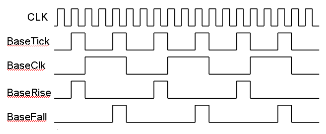
The PulseGen8 module produces a HI on its output (BaseTick) once every (clkdiv+1) master clocks. If clkdiv is zero, the the output is constantly HI. The output of the DFFRen module (BaseClk) therefore toggles at this rate. The signals BaseRise and BaseFall are asserted when, on the next master clock rising edge, the BaseClk signal will either rise or fall, respectively. These two signals are the primary timing signals for the rest of the module.
SPI Master module internal clock signals for ClkDiv = 2
//=====================================================================

// SSN Generation

//---------------------------------------------------------------------


reg [7:0] SS_reg;

reg SSN_set, SSN_reset;


Reg8 SSNREG (.Q(SSN), .D((SSN_inv == HI)? SS_reg:~SS_reg),
.en(HI), .rst(LO), .clk(~clk));


always @ (posedge clk)

begin


	if ((rst == HI)||(SS_clr == HI))


		SS_reg <= 8'd0;


	else if (SS_set == HI)


		SS_reg <= target;


	else


		SS_reg <= SS_reg;

end
The generation of the eight SSN signals is performed by setting and resetting an internal register signal in response to two command signals, SS_set and SS_clr, from the Finite State Machine controlling the SPI transfer (described later). This registered signal is latched on the rising edge of the master clock and the actual SSN output signals are inverted if necessary according to SSN_inv and then registered on the subsequent falling edge. As discussed in the section above concerning setting the ClkDiv value, one potential upgrade to the code would be to delay the changes in SSN until approximately midway between BaseClk edges.
Logically, all of the Slave Select signals should be LO when reset and should equal the value in the target vector when set. Since the actual signals (SSN) are normally logically inverted, the SSN signals equal the SS signals if the SSN_inv bit in the control register is set and the bitwise inversion of them otherwise.
Note that the output register (SSNREG) is isolated from the global reset signal. This is so that the global reset will reset the SS_reg vector and then the appropriate SSN vector will be registered on the next falling edge of the master clock. This is intended to prevent glitches on the external SSN signals since many slave devices are edge-sensitive to this signal.
//=====================================================================

// SCLK Generation

//---------------------------------------------------------------------


reg SCLK_next;


DFFRen DFF_SCLK (.Q(SCLK), .D(SCLK_next^SCLK_inv), .en(BaseTick),
.rst(rst), .clk(clk));


always @ (SS_reg or FreeRun or BaseClk or CPOL or CPHA)

begin

    if ((SS_reg != 8'd0)||(FreeRun == HI))

        SCLK_next = (~BaseClk)^(CPOL^CPHA);

    else

        SCLK_next = CPOL;

end
Recall that SCLK is basically a gated version of BaseClk, hence it is either held in its idle state (unless configured for Free Running) or allowed to track BaseClk, subject to possible signal inversion based upon the SPI Mode in use and the value of the SCLK_inv bit in the Control Register.
The effect of the SCLK_inv bit is taken care of in the output register where the non-inverted SCLK_next signal is XOR'ed with the SCLK_inv bit.
The idle condition is taken care of by noting that the idle value of SCLK is equal to the value of CPOL from the Control Register and that SCLK should be held in this state unless either at least one of the slave devices is selected (as indicated by SS_reg being non-zero) or the FreeRun bit in the Control Register is set.
If the Unless the SCLK is set to Free Running, it must be held in the state indicated by the CPOL bit from the control register unless at least one of the slave devices has been selected, as indicated by SS_reg being non-zero.
In SPI Mode 0 and SPI Mode 3, the data changes on the falling edge of SCLK. Since, within the module, data always changes on the falling edge of BaseClk, this means that in these modes we need SCLK to track BaseClk. This is done by setting the next value of SCLK to the opposite of the present value of BaseClk and scheduling that change to take effect at the same time that the BaseClk next toggles, which is controlled by BaseTick. In the other two SPI modes, data changes on the rising edge of SCLK and so we need to invert SCLK relative to BaseClk. By XOR'ing the two bits that make up the SPI Mode, namely CPOL and CPHA, we obtain the necessary logic relationship. This is describe and illustrated in more detail later when the Finite State Machine is discussed.
//=====================================================================

// Packet Length Counter

//---------------------------------------------------------------------


reg       Load;
reg [7:0] count;


always @ (posedge clk)

begin

    if ((rst == HI)||(Load == HI))

        count <= length;

    else

        count <= (BaseFall == HI)? (count -
1):(count);

end
The Packet Length Counter is a simple down counter that is loaded with the packet length at the same time that the packet data is loaded into the shift register (as indicated by the Load signal) and then allowed to decrement on each subsequent falling edge of the base clock (as indicated by the BaseFall signal).
//=====================================================================

// Data Shift Register

//---------------------------------------------------------------------


reg Shift;

wire MOSI_int;


assign MOSI = MOSI_int^MOSI_inv;
ShiftReg16DIR SR16

(

    .Sout(MOSI_int), .Sin(MISO^MISO_inv),

    .Q(packet_RX), .D(packet_TX),

    .Shift(Shift), .Load(Load),

    .Dir(Direction),

    .rst(rst), .clk(clk)

);
The Data Shift Register is a straight-forward 16-bit shift register that can shift in either direction, as controlled by the value of the Direction signal. If LO, the register shifts out the least-significant-bit and if HI it shifts out the most-significant-bit. At the same time that data is being shifted out from the transmitted packet, data is being shifted in from the received packet. The use of a fixed-length 16-bit shift register is the cause of the non-standard behavior for packet lengths other than sixteen described in the User-level Description section.
Note that any configured signal inversions controlled by MISO_inv and MOSI_inv are applied at this level.
//=====================================================================

// Transfer Initiate Logic

//---------------------------------------------------------------------


wire launch;


FireAndAcknowledge FIRE

(

    .Q(launch), .Fire(initiate), .Ack(busy),

    .rst(rst), .clk(clk)

);
The FireAndAcknowledge module is essentially a sophisticated RS flip-flop used to perform simple handshaking in a manner adopted from common practice in asynchronous logic design. The User asserts the initiate signal at a time of their choosing, but the SPI module may not be able to immediately act upon it. Furthermore, the User may relaxe the initiate signal before the SPI module is able to do so. Therefore this module captures that information and continues to assert the launch signal, which is the SPI's true initiation command, until such time that the SPI itself acknowledges that that it has responded to the command by asserting the busy signal.
It should be noted that the FireAndAcknowledge module is more than just an RS flip-flop and the description given above is a bit simplistic. The documentation for this module, which is in the support.v file, should be consulted for more information.
//=====================================================================

// Primary FSM

//---------------------------------------------------------------------


parameter

    S_IDLE    = 2'd0,

    S_SYNC    = 2'd1,

    S_COMMIT  = 2'd2,

    S_RUNNING = 2'd3;


reg [1:0] State, Next_State;


always @ (posedge clk)

begin

    if (rst == HI)

        State <= S_IDLE;

    else

        State <= Next_State;

end


// FSM State Transition Definitions

always @ (State or launch or length or count or CPHA or BaseRise or BaseFall)

begin

    case (State)

        S_IDLE: // Capture the initiate flag

            begin

                Shift = LO;

                if ((BaseRise == HI)&&(launch == HI))

                    begin

                        Load = HI;

                        busy = HI;


SSN_set = (CPHA == HI)? HI:LO;

                        SSN_reset = LO;

                        Next_State = S_COMMIT;

                    end

                else

                    begin

                        Load = LO;

                        busy = LO;

                        SSN_set = LO;

                        SSN_reset = HI;

                        Next_State =
State;

                    end

            end

        S_COMMIT: // Schedule the SSN assertion

            begin

                Shift = LO;

                Load = LO;

                busy = HI;


SSN_set = ((CPHA == LO)&&(BaseFall == HI))? HI:LO;

                SSN_reset = LO;


Next_State = (BaseRise == HI)? S_RUNNING:State;

            end

        S_RUNNING:

            begin

                Shift = BaseFall;

                Load = LO;

                busy = HI;

                SSN_set = LO;

                if (count == 8'd0)

                    begin
SSN_reset = (((CPHA == LO)&&(BaseFall == HI))
||((CPHA == HI)&&(BaseRise == HI)))? HI:LO;


Next_State = (BaseFall == HI)? S_IDLE:State;

                    end

                else

                    begin

                        SSN_reset = LO;

                        Next_State = State;

                    end

            end

        default:

            begin

                Shift = LO;

                Load = LO;

                busy = HI;

                SSN_set = LO;

                SSN_reset = LO;

                Next_State = S_IDLE;

            end

    endcase

end
To summarize the event pipeline for a packet transfer, first the module is commanded to initiate a transfer, at which point is asserts its busy flag and loads the outgoing packet data into the shift register. Then the SSN signals are asserted, followed by capture/shift (or shift/capture if CPHA is HI) cycles until all of the data is transferred. Then the SSN signals are relaxed, the module returns to the idle state, and the busy flag is relaxed.
The Finite State Machine used in the SPI module is a Mealy Machine with three states, {S_IDLE, S_COMMIT, S_RUNNING}, that controls five signals, {Load, Shift, busy, SSN_set, SSN_reset}. State transitions are dictated by one static signal {length} and four dynamic signals, {launch, count, BaseRise, BaseFall}. Of the dynamic signals, launch and count determine what transition will be made while BaseRise and BaseFall determine when that transition will occur. An additional static signal, CPHA, is used in conjunction with the others to determine the outputs in each of the states.
To understand the above code, it is helpful to study the relative timing of the signals in the various modes, as shown in the following diagram.
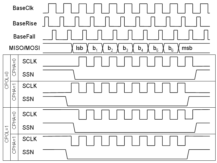
SPI Master module output signal timing
As mentioned previously, the design of the SPI module is centered on the fact that data changes only occur on the falling edge of the base clock. The timing of the SCLK and SSN signals are adjusted accordingly. In particular, note that if CPHA is LO that SSN as asserted and deasserted on the falling master clock edge just after the falling edge of BaseClk whereas if CPHA is HI then these events are advanced to the falling edge of the master clock just after the previous rising edge of BaseClk. This also requires that SCLK be advanced by one-half clock cycle, which is accomplished by a simple inversion. Similarly, the only difference if CPOL is HI versus LO is that the polarity of SCLK is changed. The combined effect is that the XOR of CPOL and CPHA determine the needed polarity of SCLK, as reflected in the SCLK Generation Code discussed previously.
The state machine normally dwells in the S_IDLE state until it detects that the launch signal has been asserted, where upon it waits until the rising edge of the BaseClk to move the machine to the S_COMMIT state where it remains for one BaseClk cycle before moving to the S_RUNNING state.
The SSN signals are asserted either on the rising edge of BaseClk concurrent with moving from S_IDLE to S_COMMIT or on the falling edge of BaseClk subsequent to moving into the S_COMMIT state, depending on the value of CPHA. Dealing with this shift in when SSN is asserted is the reason for the existence of the S_COMMIT state, though it is not the only way to deal with it.
Once in the S_RUNNING state, the FSM dwells there until the Packet Length Counter reaches zero, at which point it moves back to the S_IDLE state on the next falling edge of BaseClk. The deassertion of the SSN signals is scheduled either on the rising edge of the BaseClk between when the counter (which changes on the falling edge of BaseClk) reaches zero and when the FSM returns to the S_IDLE state or on the same edge as when it returns to the S_IDLE state, depending on the value of CPHA.
//=====================================================================

// Test Output Assignments

//---------------------------------------------------------------------


assign Test8[7] = BaseTick;

assign Test8[6] = BaseClk;

assign Test8[5] = SSN_set;

assign Test8[4] = SSN_reset;

assign Test8[3] = count[0];

assign Test8[2] = launch;

assign Test8[1] = State[1];

assign Test8[0] = State[0];
The test output assignments are somewhat arbitrary and reflect, more than anything, the latest set of signals that was used for debugging purposes. In theory, these outputs could be removed and some resources saved. However, if the signals are not used at the higher level, the synthesis tool should trim the associated logic. Therefore the bus is kept intact and ported in order to facilitate future development efforts.