RS-232 SERIAL COMMUNICATIONS
(Last Modified: 04 November 2010 06:09:02 PM )
This page is intended to give a brief overview of RS-232 serial communications with enough technical depth to understand the implementation of the RS-232 modules on the DE248 Drive Electronics.
Serial communications using the RS-232 protocols dates back to 1962 and the early days of digital communications and, as such, some of the terminology used reflects devices and concepts that, themselves, have long disappeared. None-the-less, the terminology still persists and it is very easy to get hopelessly confused unless you have a basic understanding of what that terminology originally referred to.
A useful source for more information is Maxim App Note #83.
Another useful overview can be found at the TALtech website.
Yet another can be found at CAMI Research.
Be aware that even these pages are not in complete agreement on the terminology used. Always keep this in mind when reading anything (including this page) regarding RS-232.
The RS-232 standard defines both the electrical and the communications protocols for point-to-point communications between a "host" system and a "peripheral" system. The host is known as a DTE - Data Terminal Equipment - while the peripheral is known as a DCE - Data Circuit-terminating Equipment. Since the most common DCE was originally a modem of some type, many sources refer to DCE as standing for Data Communications Equipment.
The distinction between the DTE and the DCE, while appearing arcane, is critical and possibly the number one cause of problems when trying to understand and implement RS-232. The reason has to do with the signal names, connector pin assignments, and cables.
Probably the most common place where people encounter RS-232 today is in interfacing equipment to a computer. In this case, the names and signals nearly always refer to the subset of RS-232 signals intended for telephone modem communications. For the 9-pin D-sub connector, the signals and pin assignments are as follows:
| Pin | Signal | Name | Source |
| 1 | DCD | Data Carrier Detect | DCE |
| 2 | RD | Receive Data | DCE |
| 3 | TD | Transmit Data | DTE |
| 4 | DTR | Data Terminal Ready | DTE |
| 5 | GND | Signal Ground | N/A |
| 6 | DSR | Data Set Ready | DCE |
| 7 | RTS | Request to Send | DTE |
| 8 | CTS | Clear to Send | DCE |
| 9 | RI | Ring Indicate | DCE |
DCD: Generated by the DCE to inform the DTE that it is receiving an acceptable carrier signal from the remote DCE.
RD: Data generated by the DCE and recevied by the DTE.
TD: Data generated by the DTE and received by the DCE.
DTR: Generated by the DTE to inform the DCE that it is ready to comminicate.
GND: The signal ground
DSR: Generated by the DCE informing the DTE that it is connected to a telecommunications line.
RTS: Generated by the DTE when it wants to send data to the DCE.
CTS: Generated by the DCE, in response to receiving a signal on RTS, telling the DTE that it may start transmitting.
RI: Generated by the DCE to inform the DTE that a ringing signal is being detected on the phone line.
One common cause for problems is the natural assumption that all devices transmit their data on their Transmit Data pin. However, the names are in reference to the DTE and hence the DCE receives data on the TD pin and transmits on the RD pin.
When used as intended, the DTE and DCE are connected via a "straight-through" serial cable. Such a cable connects each pin on one end to the same-numbered pin on the other end. However, most RS-232 uses today do not involve connections to a modem, but to either another computer or, more commonly, some piece of local equipment such as a multimeter. In such situations, it is frequently necessary to use special cables that may crosslink some signals and/or loopback others. Such cables are, generically, referred to as "null modem" cables but there is no standard configuration for such a cable. As a result, it is often necessary manually test serial cables to discover their pin mappings.
Most of the above signals are specific to the handshaking needs of communicating data between two computers connected via modems over a telecommunication line. When connecting a computer to a nearby piece of equipment, things can be greatly simplified. In the most extreme case, where it is assumed that both parties (the computer and the equipment) will have no problems keeping up with the traffic, a three-wire connection is possible involving only {TD, RD, GND}. A further assumption is that neither party needs any of the other handshaking signals and that those pins can be left floating. This may be the case if the system is configured for "no flow control" but that may not be an option at one end or the other. When this is the case, it is usually possible to trick the system into carrying out communications by looping back some of the signals.
Since the DE248 does not utilize hardware handshaking, specifically because of the ambiguities mentioned above, the subject will not be explored further here.
When the data rates are sufficiently high that it is possible for one party or the other to get too far behind, there needs to be a means of regulating the flow of data. This is known as "flow control". There are two types of flow control, hardware and software. Hardware flow control uses the non-data control signals to regulate data flow. Unfortunately, the fact that the ability to regulate such flow is not symmetric has led to many computers and peripherals to adopt non-standard hardware flow control protocols. On the other hand, software flow control is much more standard but it requires "in-band signaling" meaning that control signals are embedded into the data stream and there must be a means of separating the two. The biggest issue is that the transmitted data must never be able to be mistaken for control commands. This is a real possibility if the data is transmitted as raw binary data but can be avoided if all data is transmitted using ASCII.
Another advantage of an ASCII data stream is that the communications can be easily monitored using a terminal which is very handy when debugging the system. A disadvantage is that the data throughput is lowered considerably. In general, it is cut approximately in half since it takes two 8-bit ASCII characters to represent a single 8-bit binary value. This can be improved some if 7-bit ASCII is used, but the world has so strongly settled on 8-bit bytes that the savings is seldom worth the headache. If an effort is made to make the ASCII text even more readable to a human, the penalty may be much greater.
Software flow control is also known as Xon/Xoff handshaking because of the two signals that are used to implement it. In nearly all ASCII-based Xon/Xoff protocols, Xon is the Device Control 1 (DC1) character and Xoff is the Device Control 3 (DC3) character. The hexadecimal values are thus Xon = 0x11 and Xoff = 0x13.
When one side's receive buffer is in danger of being overrun, it inserts an Xoff character into the data stream that is being sent to the other side of the connections and expects the other side to pause it's outgoing data stream. Once it has cleared sufficient room in its buffer, it then sends an Xon character to the sender allowing it to resume transmission where it left off.
On the surface, this sounds very simple and easy. In practice there are a few issues that must be carefully considered when actually implementing it. The first is that there is going to be a latency between sending an Xoff command and the other side actually halting the data stream. First off, the side generating the Xoff must insert the command into its own outgoing data stream and must wait at least until the packet presently being transmitted is finished. Then the transmission of the command itself takes time and the other side must receive, decode, recognize, and act on the command before the stream can be halted. Also, the other side will not halt a packet that has already begun being transmitted. Therefore the receiver has to be very proactive about sending the Xoff command while it still has enough room in the buffer to receive several more packets.
A much more subtle, yet very serious, issue is that both sides have to be able to transmit and receive Xon and Xoff commands regardless of their state. For instance, consider the case where Side A has issued an Xoff command to Side B. Side B halts data transmission but continues to receive data from Side A. However, Side B's buffer begins to fill up and so it sends an Xoff command to Side A and so Side A halts its transmission. Both sides have now told the other side to stop transmitting data and communications is now deadlocked because neither side can tell the other side that it is safe to resume. The solution is to require that the receiver be able to receive and process Xon/Xoff commands regardless of the status of its receive buffer and regardless of whether it has told the other side to halt transmission. Similarly, the transmitter is required to be able to transmit Xon/Xoff commands regardless of whether it has otherwise halted data transmission.
Related to this issue is that Xon/Xoff commands should not even be placed into the receive or transmit buffers because they should be acted upon as expeditiously as possible.
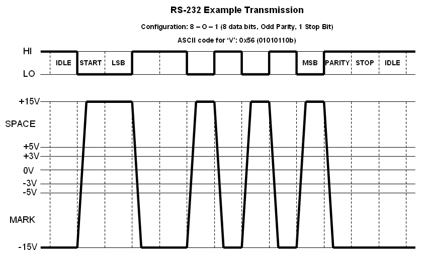
The RS-232 protocol defines two signal levels, called a "mark" and a "space" (terms that date back to the early days of telegraphy). In digital logic terms, a "mark" is a logic HI while a "space" is a logic LO. To transmit a mark the transmitter outputs a voltage between -5V and -15V. To output a space, the transmitter outputs a voltage between +5V and +15V. The receiver, in order to provide a 2V noise margin, recognizes any signal less than -3V as a mark and any signal greater than +3V as a space.
Since modern digital electronics are almost universally unipolar and at much lower voltage levels, dedicated RS-232 transceiver chips, such as the Maxim MAX-3386E, are used to translate between the system's native digital signal levels and the RS-232 signaling levels. However, many designers choose to eliminate this added cost and complexity and use the native signal levels directly. This can cause problems if such a system is connected to a system using a compliant transceiver since a signal level of 0V has an undefined logic value. Fortunately, most RS-232 transceivers discriminate between mark and space at a voltage in the neighborhood of 1V to 2V to allow them to be compatible with TTL signaling levels directly.
Note that the voltage polarity of the RS-232 signal levels is opposite from what is commonly found in digital circuitry today. This is a common source of confusion.
Communication using RS-232 is packetized meaning that data is broken into pieces and then each piece is transmitted separately. In almost all cases, RS-232 data is sent one byte at a time. The standard packet consists of one or more start bits, the data (sent lsb first), an optional parity bit, and one or more stop bits. Both parties must be configured for the same packet details.
Between packets, the transmitter holds the data line in the idle state, which is a mark. The start bits are spaces while the stop bits are marks. The parity bit is a simple form of error-detecting code in which the parity bit is set to force the overall number of marks in the packet (exclusive of the start and stop bits) to be either even or odd.
The term "baud rate" is regularly abused so, like nearly everything else related to RS-232, it is important to try to figure out what was meant as opposed to what was stated. The baud rate refers to the number of possible signal transitions per second that occur in a communications channel. Each such signal is known as a symbol, so one definition of "baud" would be "symbols/second". For normal binary communications, there is one potential signal change for every bit that is transmitted (i.e., each symbol represents one bit) and hence the baud rate and the bit rate are the same. This special case leads many people to conclude that baud rate and bit rate are always the same. However, not all digital communication systems are set up this way. In fact, because of the bandwidth filters used, the number of signal transitions on a standard telephone line is limited to around 2400 per second. To permit higher bit rates, the modem takes several bits and encodes them into a single symbol. One simple and early way to do this was to take each group of four bits and encode them, as a group, into one of sixteen possible tones. Thus it was possible to still transmit at a rate of 2400 baud (symbols per second) but each symbol conveyed four bits of information resulting in a bit rate of 9600 bits/sec.
So is it incorrect for manufacturers to refer to a 9600-baud modem? Yes and no. Remember, there are two communication channels involved - the one from the computer to the modem and the one between the modems involving the telephone line. If the 9600-baud figure is referring to the binary channel between the computer and the modem, then it is completely correct. From a practical standpoint, this is the rate that the consumer is concerned with, and so it is very arguably the correct one to specify.
But now we need to take a closer look at "bit rate" and what it really means? For example, given that the computer is transmitting 9600 bits of information each second, does that mean that we are transferring 9600 bits of data each second? The answer is "no" because not all of those bits carry information related to our data; in particular, we have the start, stop, and parity bits. These carry information, but not about the data we are trying to transfer. They carry information related to the overhead requirements of our signaling protocol. For the example used earlier where we had 8 data bits, 1 parity bit, and 1 stop bit, we have a total of 11 bits that are transmitted (we must include the start bit as well) for every 8 bits of data. Hence, if we were using a 9600 baud modem, our maximum data rate (which would only be achievable if there were never any idle bits) would be about 6981 bits/second.
As a useful rule of thumb, dividing the baud rate by ten gives the maximum data rate in bytes per second. This is because most serial communications are set up for 8-N-1 which requires that ten bits be transmitted for each byte of data.
The RS-232 protocol is an asynchronous protocol, meaning that each side has its own clock signal and that there is no true synchronization between the clocks on the two sides of the channel. Hence, if the transmitter's clock is running too fast or two slow relative to the receiver's clock then there is the possibility that the receiver will capture the data on the line thinking it is the value for a particular bit when in reality it is for either an earlier bit or a later bit. This is known as a "framing error".
Ideally, the receiver would like to sample the incoming data just prior to when it starts to change for the next symbol. This gives the greatest amount of time for the signal for the present symbol to settle and become stable. However, this invites problems if the transmitting clock is a little bit too fast because very quickly the situation will arise where the signal is already starting to change before the receiver samples the state for the present symbol. Therefore, the best situation is to sample each symbol as close to the center of the symbol's duration as possible. This provides the most protection against the other side's clock being either too much faster or too much slower and, since the connection is bidirectional, it is safe to assume that the sender's clock, relative to the receiver's clock, will be too fast for one side and too slow for the other.
So how accurate do the oscillators on each side need to be? That's actually a question that is easier to ask than to answer because oscillators are not characterized by a single "accuracy" parameter. For simplicity, we will assume that they are and that a particular oscillator runs at a constant and stable frequency that is within some accuracy tolerance of its designed frequency. In particular, we are ignoring such effects as short-term drift and edge jitter which refers to the random cycle-to-cycle period fluctuations. Notice that we are also assuming that the boundaries between symbols are infinitely narrow - in general there can be a significant amount of time required for a symbol to change from one level to another before it is safe to sample it.
To simplify the problem, let's refer all timing considerations to the receiver's oscillator and assume that it is running perfectly. In general, the receiver has to determine the "middle" of the start bit but in practice it can only approximate this by sampling the input signal and waiting until it senses a change from the stop/idle state to the start state from one sample to the next. The actual beginning of the start bit is not detected and is only known to have occurred somewhere between the two samples. It may have occurred so close to the first sample that we can assume that is where it did occur or, similarly, it may have occurred so close to the second sample that we can assume it occurred there. In the case where the transmitter's oscillator is running fast, the worst case scenario is that we just missed detecting the start of the start bit with the first sample while the worst case scenario for a slow transmission clock is that we barely caught the start of the start bit with the second sample. Thus we will perform the analysis twice, making the appropriate worst case assumption.
We will assume that both the sender and the receiver use oscillators that are nominally N times the baud rate. We will further assume that, as stated above, the receiver's oscillator is "perfect" with a period of T0 and that the sender's oscillator has a period of T. Finally, we will assume that our transmission packet consists of P symbols concluding with a final stop bit. Our reception algorithm calls for the receiver to waits until it senses the start of the start bit and then wait another B clocks before sampling the P symbols in the packet at a rate of once every N clocks. This means that the final stop bit is sampled (B+N(P-1))T0 seconds after the start of the start bit was detected.
For the worst case when the transmitter's clock is running fast, the final stop bit must be sampled before the stop bit expires, which occurs NPT seconds after the start of the start bit, which could have occurred as early as one full receiver clock period before being detected, so the end result is the following inequality:
(B+N(P-1))T0 < - T0 + NPT
Solving for maximum ratio of the period of the slower clock to the faster clock, which in this case is T0/T, we have
T0/T < NP/((NP-(N-(B+1)))
Pulling out the dominant terms, this becomes
T0/T < 1 + (1/P)[(NP-(B+1)P)/(NP-(N-(B+1)))]
Conversely, for the worst case when the transmitter's clock is running slow, the final stop bit must be sampled after the stop bit begins, which occurs N(P-1)T seconds after the start of the start bit, which could have occured as late as the moment it was actually detected. The end result this time is the following inequality:
(B+N(P-1))T0 > N(P-1)T
Again solving for the maximum ratio of the period of the slower clock to the faster clock, which in this case is T/T0, we have
T/T0 < (B+N(P-1))/(N(P-1))
Again pulling out the dominant terms, this becomes
T/T0 < 1 + (1/P)[(B/N)(P/(P-1))]
Notice that, in both cases, the dominant part of the expression is roughly 1 + 1/P. This reflects the fundamental limit that the data streams can't drift more than one clock cycle every P clocks or, if you look closely, it is really closer to 0.5 clocks every P clocks. To see this, assume that B is roughly N/2 and that N is very large.
In order to use the above results, we have to recognize that we must satisfy both constraints simultaneously, therefore, for a given set of parameters {P,N,B}, we must use whichever expression results in a smaller limit for the ratio of the slower oscillator to the faster one. Then, for a given choice of {P,N}, we can select the choice of B that results in the loosest constraint. In general, we can expect the following trends:
Larger values of P will require better oscillators.
Smaller values of N will require better oscillators.
The best value of B will be somewhere near N/2.
Before we construct a table of oscillator tolerances, we need to recognize that our expressions above give the limit on the ratio of the period of the slower oscillator to that of the faster one. Since both oscillators have a tolerance, which we will assume are identical (and this may not be a good assumption if, for instance, one side of the connection is an RC-based microcontroller and the other is a PC) with tolerance of "tol". Our expression above therefore needs to cover the case when the fast oscillator is at one side of the tolerance band and the other is at the opposite side. Thus we have:
[(1+tol)Tnom]/[(1-tol)Tnom] = 1 + (2*tol)/(1-tol)
Our two inequalities then become
tol/(1-tol) < (1/(2P))[(NP-(B+1)P)/(NP-(N-(B+1)))]
and
tol/(1-tol) < (1/(2P))[(B/N)(P/(P-1))]
The following is a table giving the required oscillator accuracies, in ppm, and optimal values of B for various values of N and P
| N | B | P=9 | P=10 | P=11 | P=12 |
| 4 | 1 | 15385 | 13699 | 12346 | 11236 |
| 8 | 3 | 22900 | 20408 | 18405 | 16760 |
| 16 | 7 | 26615 | 23729 | 21407 | 19498 |
| oo | oo/2 | 27027 | 24390 | 22222 | 20408 |
So how does this relate to real systems? Obviously it is reasonable to expect oscillators with tighter performance tolerances to cost more just as it is reasonable to expect manufacturers to want to use the least expensive parts that will meet the performance needs of the system being designed. Crystal oscillators are commonly available with accuracy specifications anywhere from about 2 ppm to around 200 ppm. Circuits using RC oscillators, which are commonly found in simple and/or very cost-sensitive embedded applications, may be more like 2% (20000 ppm).
However, the intrinsic accuracy of the oscillator is not the only consideration. If the clock is derived from a higher speed system clock, the ability to generate the desired RS-232 clock is limited by the resolution of the system clock.
As with nearly all engineering decisions, this choice involves tradeoffs. We would like to use as small a value for N as possible to reduce complexity, EMI issues, and power dissipation while we would also like to use a large value for N to improve performance. The question is really how good does it need to be to be good enough? If we want to have a good chance of being able to work with systems using RC oscillators having tolerances in the 2% range, then we can see that a value of N=16 looks pretty good, although it may not work for packet sizes greater than 12. However, we can also see that even extremely large values of N will not provide much margin at this packet length and, if we want to operate there, we probably need to require better oscillators. We can also see that N=16 puts us pretty close to the limit of performance and any better performance obtained by using larger N values is probably not worth it, especially since there are a number of issues that we have ignored and, before going for extreme performance in this regard we should look at the others more closely (which we will not do here).
If we want to use N=16 at a symbol rate of 115,200 baud, then we need an oscillator that is 1.843200 MHz. At first glance you might assume that we might have to settle for something that is simply close to this, but because RS-232 communications at this speed using this multiplier are so common, this is actually one of several "odd" standard crystal oscillator frequencies that are widely available at low cost.
In the DE248, a baud16 clock is generated that is, ideally, 1.843200 MHz. However, as stated previously, the ability to achieve this is limited by the resolution of the system master clock. For the 50 MHz oscillator on the Digilent D2 board, this resolution is 20 ns, therefore the closest we can get to the nominal period of 542.535 ns with a simple clock divider is 540 ns (with up to 200 ppm of additional uncertainty exclusive of jitter and other such issues). The result is ~5000 ppm mismatch relative to a perfectly accurate oscillator on the other end.
One game that could be played (although we won't do it here, yet), is to tweak the baud16 clock so that it is not at a uniform frequency in order to achieve better average performance over the length of one packet or, even better, over the length of one symbol. For instance, at 115,200 baud, the primary goal is for sixteen cycles of the baud clock to be as close to the nominal 8680.556 ns symbol period as possible. With a resolution of 20ns, that can be achieved very closely since 8680 ns would match it within 64 ppm, making the oscillator's intrinsic accuracy the dominant error. Using a uniform baud16 clock at 540 ns per cycle, we would have a baud symbol period of 8640 ns. In order to make up the additional 40 ns, we need two of those 16 clocks to be extended by one cycle. This is actually a simple thing to do by simply extending every eighth clock and a future revision of the DE248 will likely incorporate it.