Exam #2 Review
(Last Modified: 04 November 2010 06:11:46 PM )
Date of exam: 03 Apr 03
Topics Covered
Exam Format and Guidelines
The exam will be closed-book and closed note. At least 1/4 of the points on the exam will be from the following problems verbatim. Not all of these problems are trivial and might take quite a bit of time to solve the first time. But if the exam is the first time you are attempting to solve the problem, that will be the result of a choice you made with full knowledge of the potential consequences. In other words, ignore this review sheet at your own risk.
The exam will consist of a number of multiple choice or short answer questions followed by problem solving questions. The focus is on the fundamental concepts and your grasp of them. I am not looking for you to be able to solve complex problems involving lots of algebra within the framework of a two hour exam. If you are getting bogged down in a lot of algebra, then take a step back and look for an easier way - because it almost certainly exists. I am looking for you to be able to apply the fundamental concepts to simple problems in a manner that demonstrates that you would know how to proceed if faced with a more formidable circuit. To that end, I give substantial partial credit if you can describe how to go about solving a particular problem - keep this in mind if you are running out of time. Also keep in mind that if you spend all of your time on Question #3 and don't get to Question #4, 5 or 6, that I cannot give partial credit for problems you didn't even attempt. Read through the entire exam and answer those questions you know how to tackle first. Then at least start all of the other problems by drawing the appropriate circuit diagrams and setting up the problem solution.
I believe firmly in partial credit - but I can only give it if there is sufficient evidence upon which to base it. If you simply write down an answer, then you have just declared that you are looking for all-or-nothing grading on that problem - and that is probably what you will get. Similarly, if your "work" is merely a bunch of numbers and equations fragments scribbled in random places on the page such that your reasoning and method is not clearly visible then you will get very little partial credit.
Unless specifically stated otherwise, assume that all answers are to be supported. This may be in the form of equations and mathematical manipulation or, if appropriate, through a logical line of reasoning. Just writing down a memorized result will not get full or even most of the credit - though certainly it will get considerably more credit than if no answer at all is given.
The chart on page 601 of the text will be reproduced on the exam for your reference. As before, the basic equations for the transistor parameters (such as gm, re, rpi and so forth) will NOT be placed on the reference sheet. Neither will the relationship between f_t and the device capacitances. To remember this one just remember that in order to determine a frequency you need an RC time constant and w = 2PI*f = 1/(RC). The C is the sum of the two capacitances that characterize a transistor, namely Cpi and Cmu, and the R is the basic resistive transistor parameter - the transconductance (which is 1/resistance). Therefore f_t = gm/(2PI(Cpi+Cmu)). Make the effort to know this relationship on exam day. After that, look it up if necessary.
Review Problems
1) All homework problems. Be sure that you understand the principles behind the solutions for each. Many are of reasonable difficulty for exam questions and you can count on some of the exam problems either being homework problems or being closely related to homework problems. Certainly long homework problems will not be on the exam in their entirety - but portions of them might be.
2) The Review for Exam #1 and Exam #1 itself. If you had difficulty on that exam and have failed to correct the deficiencies identified, do not expect to be able to ignore those deficiencies and somehow do well on the Final. Continuing to neglect those issues is done at your own peril.
3) List the relative performance of Class A, B and AB amplifiers with respect to Power Efficiency and Total Harmonic Distortion.
4) If designing an amplifier for a battery powered application, what type of amplifier would probably be used as a starting point?
5) If designing a high fidelity audio amplifier, what type of amplifier would probably be used as a starting point?
6) In a Class AB amplifier, if improved linearity is needed, what typically suffers as a result?
7) In a Class AB amplifier, if the total harmonic distortion is much better than the specified goal, what might the designer elect to do?
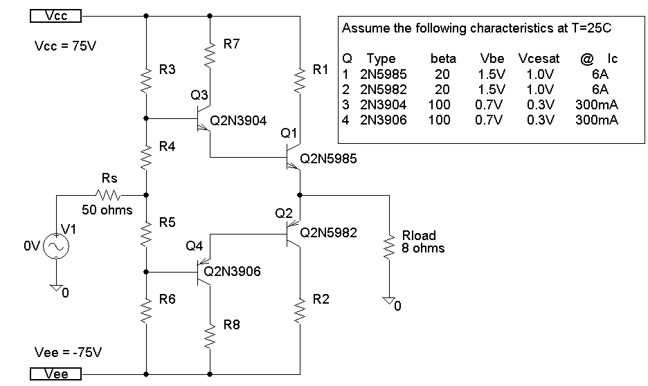
Circuit for set of questions below schematic:
An amplifier intended to deliver up to 250W to an 8 ohm speaker is to be designed using the above schematic.
1) What is the maximum value that R1 and R2 can have if the amplifier is to be able to deliver 250W to the load?
2) What is the minimum value that R1 and R2 can have if the amplifier is to limit at no more than 500W delivered to the load?
3) What is the base current into the output transistors at 250W delivered to the load (assume constant beta)?
4) What is the maximum value that R7 and R8 can have if the base drive transistors (Q3 and Q4) are to be able to deliver the necessary current to the output transistors at 250W delivered to the load?
5) What is the base current into the base drive transistors at 250W delivered to the load (assume constant beta)?
6) What is the base voltage on Q3 if the instantaneous power being delivered to the load is 250W?
7) What is the maximum value of R3 if the base current in Q3 is to be no more than 5% of the current in R3 when the amplifier is delivering 250W to the load?
8) What is the base voltage of Q1 when the collector current is 6mA? Assuming an output voltage of zero (meaning that the lower transistor, Q2, is also conducting 6mA).
9) What is the base voltage of Q3 when the collector current in Q1 is 6mA? Assuming an output voltage of zero (meaning that the lower transistor, Q2, is also conducting 6mA).
10) Using the value of R3 found in question 7, what is the necessary value of R4 if the output transistor is to conduct 6mA in the absence of an input signat (i.e., when V1 = 0V)?
11) Assuming constant betas, what is the power efficiency of this amplifier when delivering 250W to the load? Assume that the limiting conditions found in all of the above questions are adhered to, in particular the constraint outlined in question 7.
Sample Multiple Choice Questions
1) What are the two primary metrics used to describe the performance of a power amplifier?
Linearity and power gain.
Crossover deadband and total harmonic distortion.
Power efficiency and crossover deadband.
Total harmonic distortion and power efficiency.
2) For a given amplifer, which of the following do you expect to be true as the amplitude of a sinusoidal input signal is increased (without saturating any transistors)?
Distortion due to crossover deadband will decrease.
Average power delivered to the load will decrease.
Power efficiency will remain constant.
Total harmonic distortion will get worse.
3) As the temperature increases, what will happen to the base-emitter voltage of a given transistor?
It will increase regardless of the collector current.
At the same collector current, it will decrease.
At the same collector current, it will increase.
Nothing - base-emitter voltage is independent of temperature.
4) Power efficiency is defined as which of the following?
Power dissipated in the load divided by the power dissipated in the output stage of the amplifier.
Power dissipated in the load divided by the total power supplied by the power supplies.
Decreasing gain with increasing frequency.
First increasing and then decreasing gain with increasing frequency.
5) Power efficiency is generally not addressed in small signal amplifiers for what reason?
Linearity is always more important the power efficiency.
The power level is generally small enough that a poor power efficiency is not a serious concern.
Nothing can be done about it since it is dictated by the amplifier configuration used..
The power efficiency of small signal amplifiers is inherently high - only power amplifiers suffer from low power efficiencies primarily because of the low betas that typify power transistors.
6) What is the primary reason that most Class A amplifiers have poor power efficiencies?
Because all of the transistors are always maintained in the active region and hence significant power is being dissipated even in the absence of an input signal.
Because Class A amplifiers are designed to deliver very high power to a load.
Because the frequency response of a Class A amplifier necessitates higher bias currents than other amplifier classes.
Because the supply voltages must be at least four times greater than the maximum input signal if Class A operation is to be maintained.
7) Which of the following is true regarding the power dissipated in an output transistor?
It increases with increasing output voltage.
It increases with increasing collector current.
It may actually decrease as both output voltage and collector current increase.
It may be assumed to be constant in a Class A amplifier.
8) What is the defining characteristic of a Class B amplifier?
The output transistors are complimentary types (i.e., both an NPN and a PNP are used)
For large input signals, both output transistors are turned on.
The power efficiency is worse than a similar Class A amplifier.
For input signals below some critical value, the output transistors are cutoff.
9) The output configuration of the basic Class B and Class AB amplifier is also known as what?
Push-Pull Amplifier.
Totem Pole Amplifier.
Criss-Cross Amplifier.
Both A and B..
10) What is the basic meaning of Total Harmonic Distortion?
The non-linearity that arises due to non-constant gain of the amplifier
The amount of power that appears in the harmonic components as a percentage of the power appearing in the fundamental.
The amount of crossover distortion.
The sum of the voltages of the harmonics divided by the voltage of the harmonic.